Research - (2023) Volume 11, Issue 3
Investigation of A Very Sensitive Refractive Index Sensor Based On Waveguide Tm Mode Resonance and Design of a Plasmonic Sensor
Hamid Abbasi*Received: Mar 30, 2023, Manuscript No. ijcsma-23-93666; Editor assigned: Apr 01, 2023, Pre QC No. ijcsma-23-93666 (PQ); Reviewed: Apr 08, 2023, QC No. ijcsma-23-93666 (Q); Revised: Apr 14, 2023, Manuscript No. ijcsma-23-93666 (R); Published: Apr 20, 2023, DOI: 10.5281/zenodo.8046713
Abstract
This study proposes a highly sensitive refractive index sensor based on the TM wavelength resonance excited in a structure of a plasmonic sensor. The results show that the resonance wavelength will shift significantly with increasing and changing the refractive index, which shows that this method can be used to understand the resonance wavelength and refractive index. Based on this approach, the sensing characteristics, including the sensitivity and the Figure of Merit (FOM) and the Q quality factor, have been investigated, where the sensor sensitivity has reached 1165 nm / RIU. Compared to plasmon surface resonance sensors, which are based on a similar structure, the proposed sensor can achieve a more flexible range of wavelengths and a wider range of refractive index. Therefore, this method has tremendous potential for use in various fields of measurement, such as biochemical analysis and medicine, and can find useful applications in measurement systems and integrated circuits. Also, all the diagrams obtained in this research have been drawn using MATLAB program.
References
Blog | Real Estate in Australia Blog | Real Estate in Germany Car Insurance in USA Blog | Real Estate in Greece Casino Sites in Indonesia Blog | Real Estate in Indonesia Find Lawyer in Virginia Blog | Real Estate in India Casino Sites in India Blog | Real Estate in Malaysia Find Lawyer in Utah Blog | Real Estate in Philippines Best Betting Sites in Australia Blog | Real Estate in UK Casino Sites in Ethiopia Blog | Real Estate in USA Find Lawyer in Texas Blog | Real Estate in Croiatia Blog | Real Estate in Balkans Blog | Real Estate in BrazilKeywords
Plasmonics; Surface Plasmon Polaritons; Metal-Insulator Metal; Refractive Index Sensor.
Introduction
Surface Plasmon Resonance (SPR) can generate a strong electromagnetic field enhancement on the surface of a metal structure, and is very sensitive to the surrounding environment. Therefore, SPR can be applied to numerous fields such as absorption enhancement [1,2], magnetic field enhancement [3,4], photo catalysis [5–10], THz oscillation [11–13], Fano resonance [14–17], Surface Enhanced Raman Scattering (SERS) [18–21], sub-wavelength lithography [22,23], and Refractive Index (RI) sensors [24–29]. For refractive index sensors based on SPR, the resonance is excited mainly in two modes, the angular mode (at fixed wavelength) and the spectral mode (at fixed angle) [30,31]. If the light beam is in a direction where the incidence angle is fixed and the spectrum of the reflectance is probed, is called the spectral interrogation configuration and if the light beam is in a direction in which the wavelength of the incident light can be constant and the angle of incidence (slope of the light line) can be changed, it is called angular navigation configuration. Due to the low efficiency of continuous change of impact angle in a real system, the wavelength scanning method is preferred as a tool for faster measurement of the reflectance spectrum. Therefore, in this paper, we examined the wavelength scanning method, which simultaneously irradiated the analyte with different wavelengths, which showed obvious improvements over the angular-based refractive index measurement method. Using fixed-wavelength scanning, the reflection spectrum can be detected using a spectrometer, and the close relationship between Refractive index and the wavelength resonance position can be used to determine refractive index [32]. In the following, we examine parameters such as high transmission efficiency, high resolution, high quality coefficient, optical stability, Sensitivity (S) and Figure of Merit (FOM) so that the designed sensor displays an excellent performance with high optical resolution. Obtaining and improving these parameters increases the speed of information processing in optically integrated circuits.
Structural Model and Theory Analysis
The two-dimensional schematic view of the proposed plasmonic refractive index sensor consisting of two waveguides and five cavities with different dimensions and characteristics is shown in Figure 1. Two plasmonic waveguides have a height of w1 = 50 nm. A cavity with a height of w2=62 nm and a length of L1=264 nm is located in the middle of two waveguides.

Figure 1: Two-Dimensional Image of a Plasmonic Sensor.
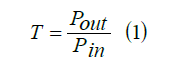
The two cavities at the top have a height of w3=220 nm and w4=100 nm, and a length of L2=100 nm and L3=100 nm, respectively, and the two cavities at the bottom have a height of w5 =100 nm and w6 = 220 nm, respectively. Length is L4=100 nm and L5=100 nm. Two monitors, Pin and Pout, are used to measure the input and output waves. The transfer rate is calculated by the following equation:
Now, in order to measure the dimensions and coordinates of the cavities and to show a better sensor, we examine the transmission spectra with different numbers of cavities. According to Figure 2, the transmission spectrum has a higher altitude for the case where only the middle cavity is active, but for the case where all five cavities are active, it has the highest wavelength transfer.

Figure 2: MIM Waveguide Transmission Spectra with Five Cavities in Different Coordinates.
Sensor Simulation and Design Methods Using Refractive Index Measurement
The proposed plasmonic resonance behavior is investigated numerically and theoretically. For the numerical approach, we use the time domain finite difference simulation method with Perfectly Matched Layer Boundary Conditions (PML) because this method effectively reduces the numerical reflection. The uniform mesh size for the x and y directions is considered to be 8 and 8 nm, respectively, and the transmission line model is used for structural theory analysis [33,34]. Two-dimensional simulation is performed, which is infinite in one dimension. The reason for this is to reduce the simulation time and achieve the desired result. The simulation is calculated in the wavelength range of 400 nm to 1600 nm. Because the drude model can be easily integrated in time-difference finite difference simulations, we use the drude model to show the optical properties of metals in simulation:
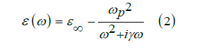
Here ɛ∞ =1 gives the medium constant for the infinite frequency, ωp = 1.37 × 10¹⁶ refers to bulk frequency for plasma, γ = 3.21 × 10¹³ means damping frequency for electron oscillation, and ω shows incident light angular frequency. The TM wave starts moving from the left and propagates in the waveguide, and the closer it gets to the output port, the lower its intensity. This beam of light that hits the metal surface from the air, never stimulates plasmon on the joint surface of the metal, unless the light beam momentum increases to match the surface plasmon momentum and obtain an intersection between two lines. This intersection reflects the resonance phenomenon and specifies the operating point at which the frequency and vector of the excited light wave and the plasmon are determined. As shown in Figure 3, the middle cavity absorbs the largest amount of TM wave. It also has the most field exchange with waveguides. When the field distribution in the structure is similar, the energy loss is reduced. To achieve the maximum field distribution in the simulated structure, all dimensions must be optimized

Figure 3: Electric Field Distribution at Resonant Frequency.
Simulation and Design of a Sensor Using Two Waveguides and a Cavity
Now we do the simulation only for the middle cavity (Figure 4).

Figure 4: Two-Dimensional Image of a Plasmonic Sensor with Two Waveguides and a Cavity.
First, to find the optimal structure, we change its length and width. The diagrams related to the change in length and width of the cavity are shown in Figure 5. We choose a height of 62 nm and a length of 264 nm for the middle cavity because the cavity in these points has a higher height and more wavelength change.

Figure 5: Diagrams Related to the Change in Length and Width of the Middle Cavity.
We now increase the refractive index of the middle cavity by a step of 0.01 from 1.14 to 1.2, which leads to a change in the resonance spectra and wavelength. We see the transmission spectrum resulting from changing the sensor refractive index in Figure 6.

Figure 6: Plasmonic Refractive Index Sensor Transmission Spectra.
To measure the performance of a plasmonic sensor, we need to consider several criteria. The first criterion is the sensitivity S, which is described as the change in resonance wavelength when the dielectric changes unit:
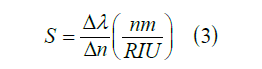
In this equation, is the change in resonance wavelength, is the change in refractive index. We see the sensitivity coefficient diagram of the plasmonic sensor in Figure 7. The maximum sensitivity for the refractive index is n=1.18 (in mode 2),which is equal to 1009 nm / RIU.

Figure 7: Plasmonic Sensor Sensitivity Coefficient Diagram.
The next criterion is the competency digit (FOM) whose equation is as follows:
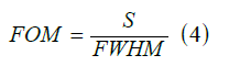
The FOM eligibility figure for the plasmonic sensor is plotted in Figure 8. According to the Figure, the maximum fitness Figure of Merit (FOM) for the refractive index is n=1.16 (in mode2), which is equal to 13.368 nm / RIU.

Figure 8: Plasmonic Sensor Figure of Merit (FOM).
The last criterion is the quality factor Q, which is obtained according to Equation 5:
We see the diagram of the quality coefficient of the plasmonic sensor in Figure 9. According to the Figure, the highest quality factor Q is for the refractive index n=1.2 (in mode1), which is equal to 16.187 nm / RIU

Figure 9: Plasmonic Sensor Quality Coefficient Diagram.
Simulation and Sensor Design Using Two Waveguides and Three Cavities
Now we add two cavities to the sensor structure and measure its performance (Figure 10).

Figure 10: Two-Dimensional Image of a Plasmonic Sensor with Two Waveguides and Three Cavities
We change the refractive index of the middle cavity with a step of 0.01 from 1.14 to 1.2 and the refractive index of the waveguides and the other two cavities remain constant. Figure 11 shows the resulting transmission spectrum, which has three modes, in the wavelength range of 400 nm to 1600 nm.

Figure 11: Plasmonic Refractive Index Sensor Transmission Spectra for Three Cavities.
We now calculate the sensitivity of the sensor, which according to Figure 12 has the highest sensitivity for the refractive index n=1.2 (in mode 3), which is equal to 1018 nm / RIU.

Figure 12: Plasmonic Sensor Sensitivity Coefficient Diagram with Three Cavities.
Next, we calculate the FIT and the quality factor Q and draw the corresponding diagrams (Figure 13). According to the figure, the highest Figure of Merit (FOM) for the refractive index is n=1.18 (in mode2) which is equal to 12.483 nm / RIU and the highest quality factor Q for the refractive index is n = 1.15 (in mode2) which is equal to with 19.089 nm / RIU.

Figure 13: Figure of Merit (FOM) And Q Coefficient Diagram of Plasmonic Sensor with Three Cavities.
Next, we change the structure of the sensor and change the coordinates and dimensions of the two upper and lower cavities (Figure 14), to measure the quality of the sensor and create a suitable structure for the sensor.

Figure 14: Two-Dimensional Image of a Plasmonic Sensor with Two Waveguides and Three Cavities.
As in the previous structure, we change the refractive index of the middle cavity by a step of 0.01 from 1.14 to 1.2 and the refractive index of the rest of the sensor structure remains constant. The transmission spectrum from the simulation can be seen in Figure 15. This spectrum, which is displayed in the wavelength range of 400 nm to 1600 nm, has three modes. Mode 3 on the right side of the chart has more flexibility than changing the wavelength.

Figure 15: Plasmonic Refractive Index Sensor Transmission Spectra for Three Cavities.
We now move on to measuring the sensor designed in Figure 14 and computing the sensitivity coefficient, quality factor Q, and the Figure of Merit (FOM). First the coefficient diagram we obtain the sensitivity, which according to Figure 16, the highest sensitivity is obtained at a refractive index of n = 1.16 (in mode3), which is equal to 1165 nm / RIU. Compared to the highest sensitivity obtained from the sensor in Figure 10, this sensor has better performance and has reached a higher sensitivity. Therefore, changing the dimensions and coordinates of the cavities has improved the sensor.

Figure 16: Plasmonic Sensor Sensitivity Coefficient Diagram with Three Cavities.
By calculating and plotting the Diagrams of the Figure of Merit (FOM) and the quality factor Q, the performance measurement of this structure is completed (Figure 17). According to the figure, the highest the Figure of Merit (FOM) for the refractive index is n=1.17 (in mode 2) which is equal to 15.128 nm / RIU and the highest quality factor Q is for the refractive index n=1.2 (in mode 1) which is equal to 24.183 nm / RIU.

Figure 17: The Figure of Merit (FOM) Diagram and The Q Coefficient Diagram of Plasmonic Sensor with Three Cavities.
Simulation and Design of a Sensor Using Two Waveguides and Five Cavities
We now design a combination of the two structures designed in Figures 9 and 13 to obtain a better and more efficient sensor (Figure 18).

Figure 18: Two-Dimensional Image of a Plasmonic Sensor with Two Waveguides and Five Cavities.
We obtain the transmission spectrum by changing the refractive index of the middle cavity with a step of 0.01 from 1.14 to 1.2 (Figure 19). Here the refractive index of the other four cavities remains constant. This stabilizes the sensor performance and improves its quality. The resulting transmission spectrum has two peaks, with the right peak having more flexibility in changing the wavelength.

Figure 19: Plasmonic Refractive Index Sensor Transmission Spectra for Five Cavities.
To analyze the structure of this sensor, we first calculate the sensitivity coefficient in the wavelength range of 400 nm-1600 nm and then draw a graph. The sensitivity coefficient diagram, as the first criterion for measuring the performance of this sensor, shows us that the maximum sensitivity coefficient obtained using the transmission spectra of this sensor is equal to 1124 nm / RIU (Figure 20).

Figure 20: Plasmonic Sensor Sensitivity Coefficient Diagram with Fine Cavities.
The next criterion for measuring the performance of the FOM sensor is obtained using Equation 4. Drawing the corresponding diagram (Figure 21), we find that the highest value of Qom is the merit (FOM), with a refractive index of n=1.15 (in case 1), which is equal to 12.395 nm / RIU.

Figure 21: The Figure of Merit (FOM) Diageram for Plasmonic Sensor with Two Waveguides and Five Cavities.
The final criterion for measuring the structure of this sensor is the quality factor Q. Using Equation 5, we draw the corresponding diagram (Figure 22). The highest quality factor Q for the refractive index is n=1.15 (in case 1) which is equal to 20.505 nm / RIU.

Figure 22: Q-Quality Factor Diagram for Plasmon Sensor with Five Cavities.
Our research on this sensor is over. With the structure that was designed and by changing the coordinates and dimensions of the cavities, we were able to study and analyze our desired sensor in different states and conditions and achieve a stable and balanced structure for making plasmonic sensors.
Conclusion
In this paper, a refractive index sensor based on TM wavelength resonance is investigated. An amplifier system connected to a plasmonic waveguide, consisting of two Metal-Insulated Metal Waveguides (MIM) with five cavities, has been designed and numerically evaluated using the Finite Deference Time Domain method. The results show that the resonance wavelength will shift significantly with increasing and changing the refractive index, which suggests that this method can be used to understand the resonance wavelength and refractive index. Next, the sensitivity coefficient and FOM competency S and Q quality coefficient are examined, in which the sensor sensitivity has reached 1124 nm / RIU and 1165 nm / RIU. This means that the sensor, due to its high resolution, can easily analyze the change in refractive index of 0.01 for materials with a refractive index of between 1.14 and 1.2. Also, all the diagrams obtained in this research have been drawn using MATLAB program. Hopefully, the proposed structure will provide guidelines for the design of Nano-sensors.
Data Availability
Data sharing is not applicable to this article as no datasets were generated or analyzed during the current study.
Code Availability
Numerical analysis of this paper is based on FDTD method.
Funding Information
This study hasn’t any financial support.
Authors’ Contributions
All authors have same contribution in the analytical and numerical calculations and read and approved the final manuscript.
References
- Cen, C., et al. "Tunable absorption enhancement in periodic elliptical hollow graphene arrays." Opt Mater Express. 9.2 (2019): 706-716.
- Lin, H., et al. "Plasmonic absorption enhancement in graphene circular and elliptical disk arrays." Mater Res Express. 6.4 (2019): 045807.
- Chen, J., et al. "Optical magnetic field enhancement via coupling magnetic plasmons to optical cavity modes." IEEE Photonics Technol Lett. 28.14 (2016): 1529-1532.
- Chen, J., et al. "Surface-plasmon-polaritons-assisted enhanced magnetic response at optical frequencies in metamaterials." IEEE Photonics J. 8.1 (2015): 1-7.
- Zhao, X., et al. "Synthesis and theoretical study of large-sized Bi4Ti3O12 square nanosheets with high photocatalytic activity." Mater Res Bull. 107 (2018): 180-188.
- Lijing, D., et al. "Construction of Z-scheme g-C3N4/CNT/Bi2Fe4O9 composites with improved simulated-sunlight photocatalytic activity for the dye degradation." Micromachines 9.12 (2018): 613.
- Yan, Y., et al. "Enhanced photocatalytic activity of surface disorder-engineered CaTiO3." Mater Res Bull. 105 (2018): 286-290.
- Zheng, C., et al. "A novel Bi 4 Ti 3 O 12/Ag 3 PO 4 heterojunction photocatalyst with enhanced photocatalytic performance." Nanoscale Res Lett. 12 (2017): 1-12.
[Google Scholar ] [CrossRef]
- Lijing, D., et al. "Facile synthesis and enhanced visible-light photocatalytic activity of novel p-Ag 3 PO 4/n-BiFeO 3 heterojunction composites for dye degradation." Nanoscale Res Lett. 13 (2018): 1-13.
- Hou, W., and Stephen B. C. "A review of surface plasmon resonanceâ?enhanced photocatalysis." Adv Funct Mater. 23.13 (2013): 1612-1619.
- Safari, S., and B. Jazi. "The role of terahertz surface plasmons in the scattering pattern of electromagnetic waves in an unstable elliptical plasma antenna." Phys Plasmas 24.7 (2017): 072112.
- Hongmei, D. U., et al. "THz plasma wave instability in field effect transistor with electron diffusion current density." Plasma Sci Technol. 20.11 (2018): 115001.
- Dongao, L. I., et al. "The instability of terahertz plasma waves in cylindrical FET." Plasma Sci Technol. 21.4 (2019): 045002.
- Wang, J., et al. "Tunable Fano resonance based on grating-coupled and graphene-based Otto configuration." Opt Express. 25.20 (2017): 23880-23892.
- Zhang, X., et al. "Refractive index sensor based on fano resonances in plasmonic waveguide with dual side-coupled ring resonators." Photonic Sens. 8 (2018): 367-374.
- Piao, X., et al. "Fano-type spectral asymmetry and its control for plasmonic metal-insulator-metal stub structures." Opt express. 19.11 (2011): 10907-10912.
- Piao, X., Sunkyu Y., and Namkyoo P. "Control of Fano asymmetry in plasmon induced transparency and its application to plasmonic waveguide modulator." Opt express. 20.17 (2012): 18994-18999.
- Liu, G., et al. "One-process fabrication of metal hierarchical nanostructures with rich nanogaps for highly-sensitive surface-enhanced Raman scattering." Nanotechnology 26.18 (2015): 185702.
- Xiang, W., et al. "Surface-enhanced Raman scattering effect of composite structure with gold nano-cubes and gold film separated by polymethylmethacrylate film." (2019).
- Yu, Meidong, et al. "Annealed gold nanoshells with highly-dense hotspots for large-area efficient Raman scattering substrates." Sens Actuators B: Chem. 262 (2018): 845-851.
- Wang, X., et al. "Investigation of surface plasmons in Kretschmann structure loaded with a silver nano-cube." Results Phys. 12 (2019): 1866-1870.
- Wang, X., et al. "Theoretical investigation of subwavelength structure fabrication based on multi-exposure surface plasmon interference lithography." Results Phys. 12 (2019): 732-737.
- Wang, X., et al. "Theoretical realization of three-dimensional nanolattice structure fabrication based on high-order waveguide-mode interference and sample rotation." Opt Quantum Electron. 51 (2019): 1-8.
- Liang, C., et al. "Tunable triple-band graphene refractive index sensor with good angle-polarization tolerance." Opt Commun. 436 (2019): 57-62.
- Liu, C., et al. "Symmetrical dual D-shape photonic crystal fibers for surface plasmon resonance sensing." Opt express 26.7 (2018): 9039-9049.
- Liu, Z., et al. "Enhancing refractive index sensing capability with hybrid plasmonic–photonic absorbers." J Mater Chem. C 3.17 (2015): 4222-4226.
- Yun, Q. P., et al. "Refractive index sensor and filter of metal-insulator-metal waveguide based on ring resonator embedded by cross structure." (2018).
- Cen, C., et al. "A tunable plasmonic refractive index sensor with nanoring-strip graphene arrays." Sensors 18.12 (2018): 4489.
- Liu, C., et al. "Mid-infrared surface plasmon resonance sensor based on photonic crystal fibers." Opt express. 25.13 (2017): 14227-14237.
- Abutoama, M., and Ibrahim A. "Self-referenced biosensor based on thin dielectric grating combined with thin metal film." Optics express 2 3.22 (2015): 28667-28682.
- Abutoama, M., and Ibrahim A. "Angular and intensity modes self-referenced refractive index sensor based on thin dielectric grating combined with thin metal film." IEEE J Sel Top Quantum Electron. 23.2 (2016): 72-80.
- Wang, X., et al. "Theoretical investigation of a highly sensitive refractive-index sensor based on TM0 waveguide mode resonance excited in an asymmetric metal-cladding dielectric waveguide structure." Sensors 19.5 (2019): 1187.
- Gierak, J., et al. "Sub-5 nm FIB direct patterning of nanodevices." Microelectron Eng. 84.5-8 (2007): 779-783.
- Wu, W., et al. "Ultra-high resolution filter and optical field modulator based on a surface plasmon polariton." Opt Lett. 41.10 (2016): 2310-2313.